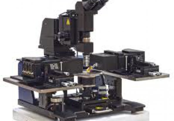
300 mm/12 inch Wafer Probing Station for mm-Wave applications
A wafer is a thin slice of semiconductor material, such as a silicon crystal, used in the fabrication or prototyping of integrated circuits (ICs) and other micro devices. A wafer probing station is the simplest and most direct method of testing un-encapsulated die (a portion/chip of a wafer).
Wafer probing is required if:
Contact Person/s
Grantholder