300 mm/12 inch Wafer Probing Station for mm-Wave applications
Model:
Wafer Probing Station for mm-Wave applications
Manufacturer:
Supplier:
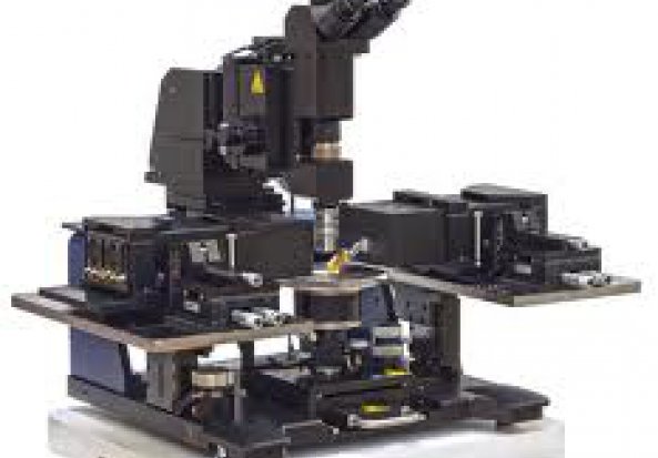
A wafer is a thin slice of semiconductor material, such as a silicon crystal, used in the fabrication or prototyping of integrated circuits (ICs) and other micro devices. A wafer probing station is the simplest and most direct method of testing un-encapsulated die (a portion/chip of a wafer).
Wafer probing is required if:
- Specification requires that dies are 100% probed or characterised.
- Select parameter testing or probing at temperature (hot/cold).
- Devices with higher performance levels are to be identified and segregated accordingly.
- A possible industry is envisioned in specialised device testing/characterisation (and modelling).
The "300 mm" provides the maximum size of the wafer that can be tested. Smaller wafers or diced wafers/dies can also be tested using this prober.
Status:
Available
Condition:
New
Category:
Other
Disciplines:
Electronic Engineering