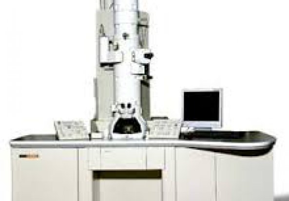
Jeol JEM 2100 Transmission Electron Microscope (TEM) Electron Microscopes
The TEM is configured to be an analytical facility to investigate and characterize the internal structure of very thin sections of material, up to around 200 nm thick depending on the atomic number of the material. The electron accelerating voltage ranges from 80kV to 200 kV, a range consistent with being about to provide basically damage free conditions for both life and material science materials. The possible characterization modes include imaging the microstructure via both bright field (transmitted electrons), as well as dark field and HAADF (scattered electrons).
Contact Person/s
Grantholder


