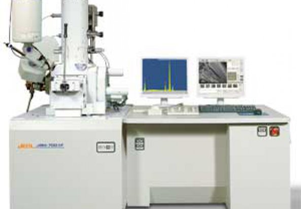
Electron nano-beam lithography JEBL-7001F Electron Microscopes
JEBL-7001F Electron Nano-beam Lithography with Four Nano Probe Electron Device Testing Station and Cantilever Probe Scanner at low Temperatures is set up for fabricating nano-electronic, nano-magnetic quantum devices, in situ transport measurement and simulteneous imaging truly at the nano-scale in a clean room area.The complete nano-spin and electronic transport measurement station (NSETMS) is designed by combining a set of four Nano-Manipulators,a high vacuum atomic force microscope (AFM) (from Kleindiek nanotachnik), an e-beam writer (Rath Elphy Quantum Electron Beam Lithography with bea
Contact Person/s
Grantholder
Title: Prof
First Name: Somnath
Last Name: Bhattacharyya
Phone: +27 11-717-6811
Email: Somnath.bhattacharyya@wits.ac.za
First Name: Somnath
Last Name: Bhattacharyya
Phone: +27 11-717-6811
Email: Somnath.bhattacharyya@wits.ac.za